
Flash Memory Manufacturing Process
Flash memory manufacturing has five stages: wafer sorting and testing, COB bonding or SMT placement, housing and assembly, marking and branding, and test and packing. Each stage has a decision attached to it that affects the product you receive — die grade is set at the first, the die format and controller package at the second, and the last is where an under-capacity unit gets caught. This page sets out what happens at each stage and what is checkable, so you can tell whether a supplier’s description of its own process is specific enough to mean anything.
The five stages
- Wafer sorting & testing Die-level screening before packaging.
- COB bonding / SMT placement Bare die or packaged part onto the PCB.
- Housing & assembly Metal, PVC or wood housing assembly.
- Marking & branding Silk-screen, colour print, laser engraving.
- Test & pack Capacity / read-write verification, then packaging.
What is decided at each stage, and how you can check it
| Stage | What happens | Decision made here | How you check it |
|---|---|---|---|
| Wafer sorting & testing | Incoming die is screened and graded before it is packaged or bonded. Grade decides field behaviour — retention and failure rate — far more than it decides benchmark speed. | Die grade and source | Ask for the sourcing breakdown on your project. |
| COB bonding / SMT placement | Bare die bonded directly to the PCB, or a packaged part placed by machine. The die format is chosen against capacity, cost target and mechanical constraint. | Die package format | TSOP (Thin Small Outline Package), BGA (Ball Grid Array), LGA (Land Grid Array), COB (Chip-On-Board), eMMC (Embedded MultiMediaCard) |
| Controller pairing | The controller is paired with the flash and configured for the target capacity and host interface. | Controller solution and package | Controller packages: QFN, 24-pin, 48-pin, COB. |
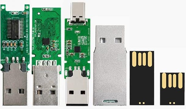
| Housing & assembly | Metal, PVC or wood housing, or the module left bare for board-level integration into your own product. | Finished product, module, or bare PCBA | Decides whether you order a finished drive, a UDP module or a semi-finished board. |
| Marking & branding | Silk-screen printing, full-colour printing or laser engraving to your artwork, chosen to suit the body material. | Print method | Approve a physical sample before bulk production. |
| Test & pack | Capacity and read/write verification before packing to bulk, retail or presentation packaging. | Acceptance criteria | Tell us the criteria you work to and we will confirm how the batch is checked. |
Die package formats
| Format | Full name | Where it is used |
|---|---|---|
| TSOP | Thin Small Outline Package | Legacy NAND package, still widely sourced for cost-sensitive builds. |
| BGA | Ball Grid Array | Higher-density package used for larger capacities. |
| LGA | Land Grid Array | Documented in our source material as Apple-component grade LGA parts. |
| COB | Chip-On-Board | Bare die bonded directly to the PCB — the basis of UDP and card production. |
| eMMC | Embedded MultiMediaCard | Managed NAND with integrated controller, for embedded designs. |
Where your order enters the chain
At the beginning — finished product
You buy a finished TF card, custom USB drive or finished module. We run the whole chain and you receive a packed product to your specification.
Partway — you finish it
You have a housing or an assembly line. Order the UDP module or the semi-finished board and take it from there.
Tell us where your product enters the chain
Send the product type, capacity, quantity and what you do in-house. We reply to business enquiries within 1 business day.
Request a quoteFrequently asked questions
How long does the process take?
Lead time depends on the configuration, the branding method and whether a new mould is needed. We confirm a schedule in the quotation against your target date rather than publishing one lead time that pretends to cover every order. See production lead time for what drives it.
Can I specify the die package format?
Yes, within what the capacity and mechanical constraints allow. We source in TSOP, BGA, LGA, COB and eMMC formats and will tell you which fits your requirement rather than defaulting.
What happens if the silicon we chose is discontinued?
It is a genuine risk — major suppliers discontinue NAND packages on their own schedule. Tell us your expected production life when you enquire and we will discuss how to plan for it.